486
Views & Citations10
Likes & Shares
A semiconductor made by binary composite is a mixture of two fundamentals as of the periodic table like; Zinc Telluride (ZnTe) is a cluster of II-VI composite semiconductor which is a combination of Zinc (Zn) from Column II and Tellurium (Te) from Column VI. ZnTe is an important semiconductor which shows energy band gap of 2.26eV. It is usually a p-type semiconductor. Zn/Te is promising material for purely green light-emitting diode. Column II-VI of periodic table the semiconductors without difficulty doped by n-type impurities other than resist p-type impurities doping.
Keywords: Thermal evaporation, Vacuum unit, Four point probe method
INTRODUCTION
In current work thin films of P-type Zn/Te of various thickness has deposited on N-type clean silicon substrate with the deposition rate 8 Å/s. The N-type silicon (Si) substrate was cleaned by the Solution of RCA in ratio of 5:1:1 of DI water, Hydrogen peroxide and Ammonium hydroxide to remove ionic, metallic and oxide native particles contamination and rinse the silicon wafer by the DI water and dry in spin rinse dryer [5]. The annealing process was done for enhance the crystallinity and plane morphology of the thin films. So thin films have kept at without annealing, annealing at 200°C and 300°C to examine the effect of recrystallization at a certain temperature. It has experimented with the purpose of decreases in resistivity exponentially as the temperature increases. Electrical properties were measured using four point probes. The distance between object and source at the time of deposition of thin films in vacuum coating was 30 cm [4,5].
EXPERIMENTAL DETAILS
Materials and methods
P-type Tellurium (Te) has been purchase from Koch-Light laboratories, Colebrook Berks England and Zinc (Zn) has been purchase since Sigma Aldrich laboratories. Single crystal N-type silicon wafer substrate was Grade prime CZ have diameter 3 inch, thickness was 380+/-25 µmicron, orientation , Resistivity was 1-10 Ω·cm and surface was particular side polished [6].
Synthesis
The Zn/Te heterostructure thin film has deposited by thermal evaporation scheme on correctly clean substrate of silicon with the dimension of 1 × 1 cm2 to begin with dirt-free the chamber and tungsten boat through acetone [7]. The Zinc (Zn) and tellurium (Te) powder with purity of 99.99% placed in a tungsten boat and start pumping unit and starts create high vacuum in chamber. Subsequent to 10-5 mbar vacuum the Te intense obliquely with temporary current gradually to electrodes and Te with different thickness (200 nm, 500 nm, 750 nm and 1000 nm using thickness ratio 1:1) have been deposited on silicon. Thickness of materials on substrate has been controlled by means of crystal monitor (“Hind Hivac” Digital Thickness Monitor Model–DTM–101).
Characterization
Structural characterization has been done through X-ray diffraction unit manufactured by Panalytical (Xpert-Pro) & and electrical properties have been considered by four point probe setup manufactured by OMEGA [2,8]. The outside morphology of films have been analysed through scanning electron microscopy. Mobility is measured by Ecopia HMS-3000 Hall measurement system.
RESULTS AND DISCUSSION
Electrical properties
Electrical I-V measurement
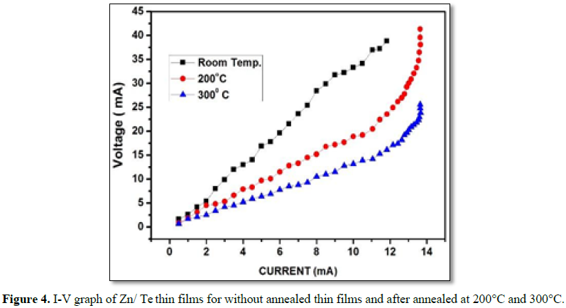
Effect of thickness vs. Voltage-Current (V-I) characterization of prepared Zn/Te thin films were also studied. The measurements were taken at room temperature for without annealing thin films, after annealed at 200°C and 300°C for 500 nm Zn/Te thin films. By Figure 4 observed that I-V curve is measured at room temperature for without annealed Zn/Te thin films which indicate linear I-V curve with ohmic contact variation at the interface between of Zn/Te and Si substrate contact which shows non-rectifying barrier potential at the interface of P-N junction contact [9]. At ohmic contact current is relative to applied voltage magnitude accordance with ohm’s law. I-V curve is obtained Linear at room temperature for without annealed thin films shows ohmic contact with typically metallic nature of Zn/Te thin films. This ohmic behaviour increase with increasing the temperature of films. At 200°C after annealing thin films clearly indicate that the thin films shows nonlinear curves after heat treatment appropriate with granular uniformity and demonstrate Schottky contact at the interface which shows rectifying behaviour of potential barrier between P-N junctions with tunnelling effect. After annealing at 300°C tellurium diffuse in Zinc and readily available Schottky barrier junction in the interface that makes alloy compound of Zinc Telluride (ZnTe). Thin films attained semiconductor nature after heat treatment [10].
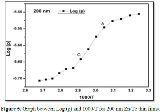
Resistivity v/s temperature relation
The effects of thickness and temperature on resistivity of the prepared thin films were studied. The measurement was occupied with remain the current constant with sweeping the voltage at dissimilar temperature [11]. It was set up that the resistivity decreases exponentially with increasing temperature for all the Zn/Te thin films which indicate that these thin films have semiconductor behavior (Figure 5).
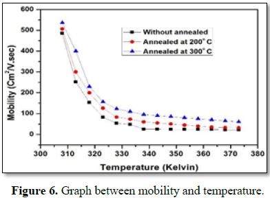
Mobility measurement
Mobility of charge carriers which is called “Hall mobility” is measured using “Hall Effect” measurement. Mobility of charge carriers exponentially decreases with increase the temperature (Figure 6). It is also observed that the mobility of charge carriers at without annealed thin films is less than the mobility of charge carriers comparatively after annealed at 200°C and 300°C. It is also observed that mobility of conduction electrons is more than the valance electrons and conduction electrons are more easily affected than valence electrons. It is also observed that with increasing the temperature, relaxation time or mean free time between charge carriers collision also increases. In XRD analysis observed that after annealing the crystal grain particle size increases and there would be better contact at the interface of Zn/Te and Si substrate due to it mean free life time of charge carriers decreases and mobility decreases with increases the annealing temperature of thin films [10].
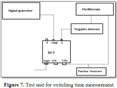
Electrical switching characterization
A P-N junction at the interface of contact Zn/Te on Si substrate works as a diode can neither turn ‘ON’ nor turn “off” instantly. It takes finite time for turning “ON” and turning “Off” which is called switching times of diode [11]. Diode has two switching time: Forward recovery time and Reverse Recovery Time. Test unit for the measurement of switching time shown in Figure 7.
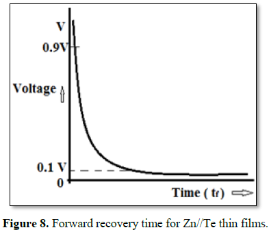
(a) Turn on time (forward recovery time) in Figure 8 shows that when diode is forward biased (turned on), voltage across it reduces. Turn on time is defined as time interval in which voltage across diode changes from 90% maximum voltage to 10% of minimum voltage.
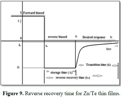
(b) Turn off Time (Reverse Recovery Time) shown in Figure 9 which indicate that when a forward biased diode is suddenly reverse biased, current does not drop to zero instantly. It takes finite time to drop to zero. This time is known as Turn off time. Reverse recovery time plays a major role in high speed switching application. For fast switching from “ON” state to “OFF” state, the reverse recovery time should be as small as possible. In Figure 9 (ts) is the storage time, when the diode is in reversed biased the positive terminal of battery repels injected minority holes and negative terminal of battery repels injected minority electrons. Therefore, current flows whose direction is from N-region to P-region (reverse current). This current is constant till all injected holes return back to their parent region P and excess electrons to N-region. This time interval (t1-to) is known as storage time (ts). After this instant current falls to reverse saturation current (I0) (I0 is due to thermally generated minority charge carriers).The time interval (t2-t1) is called as transition time (tt).
Sum of these two time intervals (ts and tt ) equals the turn off time or reverse recover time (trr) of P-N junction diode [1,8].
Structural properties
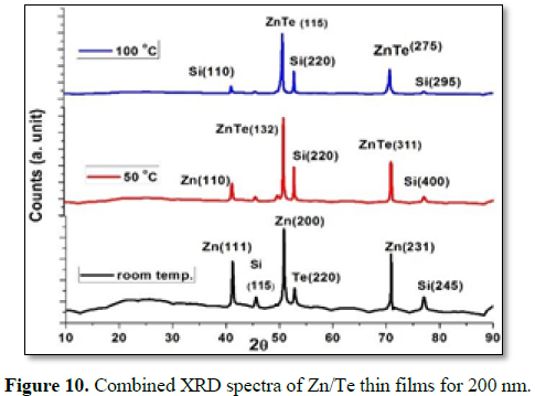
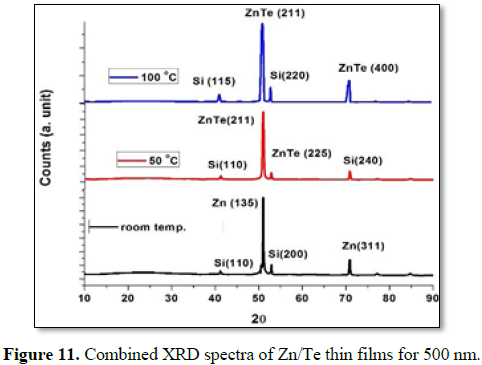
The Zn/Te thin films characterized with XRD with and without annealing. XRD pattern for 200 nm shown in Figure 10 and 500 nm shown in Figure 11. Results point out XRD peaks analogous to Tellurium Zinc at specific 2θ angle for orthorhombic face of thin films. This work confirmed that corresponding materials have been successfully deposited on substrate, Silicon and Zinc peaks are exposed whereas no peak related to “Te” appeared because of non-crystalline performance of Tellurium. Subsequent to annealing Tellurium has been merged in Zinc and relative peaks of composites of Zinc telluride starts appear. Observed peaks analysed using standard XRD pro software [12]. By XRD analysis it is also observed that with higher annealing temperature peak height increases and the peak width decreases. It has been observed that grain and crystals size increases due to growth of the peak height is the function of annealing temperature which could grow up the crystalline phase of thin films.
AFM analysis
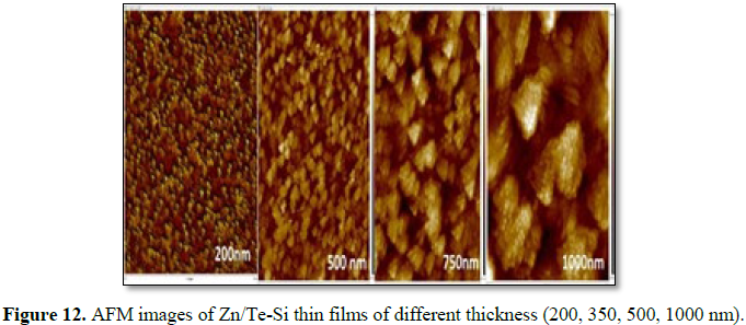
By AFM Analysis observed that crystallinity and granularity of thin films increased with increase the thickness of the Zn/Te thin films. By Figure 12 it is also noticed that by means of enhance the thickness size of the crystal and grain particles also increases. This shows that thin film grows in granular phase manner and become smoother as the thickness increased [13]. An AFM image confirms the polycrystalline nature of Zn/Te on Si thin films (Figure 12).
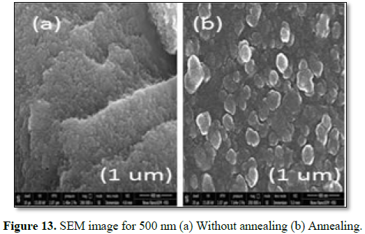
SEM analysis
The without annealing and annealing result measured by SEM images for dissimilar magnification which has decreases as of 10 µm to 1 µm which is exposed in Figure 13. These thin films visibly point out that Tellurium and Zinc full-grown on Silicon which results that large granular clusters starts to be appear with the decrease in magnification from 10 µm to 1 µm later than annealing surface morphology of thin films recrystallize. After annealing rough lumps and large bunch starts to appear in spherical shape and distributed on the whole surface. These clusters formed due to the agglomeration of particles during to heat treatment. In accordance to the SEM images it may bring to a close that thin films which are as-deposited have partially amorphous structure even as after annealing it becomes polycrystalline in nature. Without annealed thin film becomes smoother in outside morphology on the other hand after annealing minute gapes starts appear in between the granules due to diffusion of Tellurium in Zinc particles which supports our electrical studies. After annealing the amplitude of atomic vibration increases due to it crystal grain size shows large interatomic spacing between the grain particles. By SEM analysis it also concluded that grain size is increases when the annealing temperature is increasing [6,7].
CONCLUSION
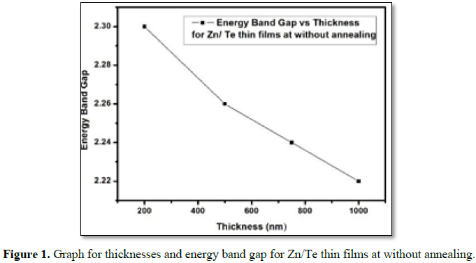
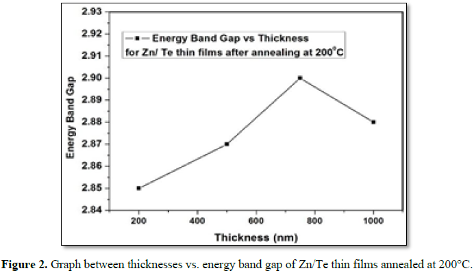
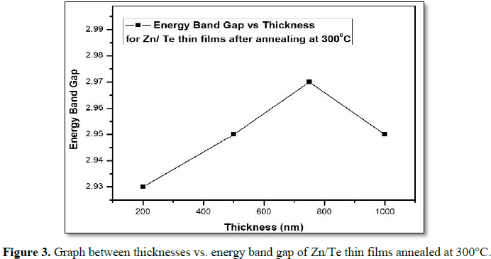
Zn/Te Thin films hetero structure of variety of thickness has been fabricated on silicon under the vacuum of about 10-5 torr, by vacuum coating unit. Energy band gap (direct) has been obtained 2.22 eV to 2.30 eV at without annealing through Four point Probe scheme which results that as we increase the material thickness, Energy band gap decreases exponentially. To find out the effect of recrystallization thin films of Zn/Te were annealed at 200°C and 300°C. After annealing it has been observed that energy band gap increases till 750 nm and suddenly decreases due to “Quantum Confinement Effect” and higher size of the grain particles and energy band gap obtained in range of 2.85 eV to 2.97 eV. Atomic force microscopy, X-ray diffraction, and scanning electron microscopy analysis are done to get complete and reliable micro structural in sequence. I-V Electrical measurements done for find out the nature of thin films. Electrical switching times study also done in forward and reverse bias after set up the devices to find out the effect of forward recovery time and reverse recovery time on P-N junction Zn/Te heterostructure which shows that reverse recovery time is product of transition time and storage time that is desirable measurement in high speed switching applications.
CONFLICT OF INTEREST
The authors declare that they have no conflict of interest.
1. Zhang B, Guo F, Wang W (2012) Synthesis and characterization of ZnTe hierarchical nanostructures. J Nanomater 2012: 1-5.
2. Prem Kumar T, Saravana Kumara S, Sankaranarayanan K (2011) Effect of annealing on the surface and band gap alignment of CdZnS thin films. Elsevier Publication Appl Surf Sci 257: 1923-1927.
3. Bowen WE, Wang W, Phillips JD (2009) Complementary thin film electronics based on ZnO/ZnTe. IEEE Device Res J 110: 183-185.
4. Ahamed JU, Begum NP, Khan MNI (2017) Property elucidation of vacuum-evaporated zinc telluride thin film towards optoelectronic devices. Indian Acad Sci 42: 1773-1781.
5. Rathod JR, Patel HS, Patel KD, Pathak VM (2013) Structural and optical characterization of zinc telluride thin films. Adv Mater Res 665: 254-262.
6. Srimathy N, Kumar RA (2017) Deposition and Characterisation of zinc telluride as a back surface field layer in photovoltaic applications. Mechanics Mater Sci Eng 2412: 312-322.
7. Hassun KH, Maki AS (2016) The structural and optical properties of zinc telluride thin films by vacuum thermal evaporation technique. J Pure Appl Sci 29: 70-80.
8. Chakraborty M (2011) Dimensional effect on optical properties of cadmium zinc telluride thin films. Int J Eng Sci Technol 3: 7402-7407.
9. Rusu IG, Prepelita P, Rusu SR, Apetroaie N, Oniciuc G, et al. (2006) On the structural and optical characteristics of zinc telluride thin films. J Optoelectronics Adv Mater 8: 922-926.
10. Alias MFA, Razooqi MA, Abdullah RA, Al-Douri AA, Alnajjar AA (2011) The influence of annealing temperature on electrical properties of thermally deposited CdTe films. 4th International Conference of Salahaddin University, Erbil 3: 18-20.
11. Kumar S, Rajpal S, Sharma SK, Roy D, Kumar SR (2017) Effect of annealing on the surface and optical properties of ZnCdS nanocrystalline thin films. Chalcogenide Lett 14: 17-23.
12. Arora S, Vijay YK (2018) Electrical, structural and optical properties of tellurium thin films on silicon substrate. AIP Conference Proceedings 1953: 030083.
13. Arora S, Jaimini V, Srivastava S, Vijay YK (2017) Properties of nanostructure bismuth telluride thin films using thermal evaporation. J Nanotechnol 2017: 1-4.
QUICK LINKS
- SUBMIT MANUSCRIPT
- RECOMMEND THE JOURNAL
-
SUBSCRIBE FOR ALERTS
RELATED JOURNALS
- Journal of Biochemistry and Molecular Medicine (ISSN:2641-6948)
- Journal of Genomic Medicine and Pharmacogenomics (ISSN:2474-4670)
- Journal of Veterinary and Marine Sciences (ISSN: 2689-7830)
- Journal of Microbiology and Microbial Infections (ISSN: 2689-7660)
- Proteomics and Bioinformatics (ISSN:2641-7561)
- Journal of Agriculture and Forest Meteorology Research (ISSN:2642-0449)
- Journal of Astronomy and Space Research